Operator Name :Mr. Biplab Saha
Operator Email :bsaha.elc@gmail.com
Operator Contact :8296200430
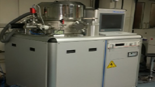
DC sputtering utilizes a DC gaseous discharge. Ions strike the target (the cathode of the discharge), which is the deposition source. The substrate and the vacuum chamber walls may be the anode. the power supply is simply a high-voltage DC source.
RF-sputtering is a suitable technique to fabricate optical planar waveguides and photonic microcavities operating in the visible and NIR regions. Sputtering techniques are widely used in industrial process because high quality films can be obtained at low temperature substrates. We have also demonstrated as the rf sputtering is a suitable technique for fabrication of dielectric microcavities and it is a cheap and versatile technique to deposit alternating layers of different materials with controlled refractive index and thickness. With these advantages, as well as the possibility to incorporating QCM, RF-sputtering process is a extremely appropriate candidate to fabricate high quality and homogeneous 1-D photonic crystals and planar waveguides.